There are five objects in the debug toolchain:
IDE -> gdb-for-target-architecture -> debugger-hw-server -> debugger-hw -> target-uC.
Here are some examples.
- IDE: e.g. Atmel Studio 6; Eclipse; IAR
- gdb-for-target-architecture: e.g. gdb-earm; gdm-nordic
- debugger-hw-server: e.g. st-util
- debugger-hw: e.g. AVR JTAGICE; SEGGER
- target-uC: e.g Atmel at2560, STM32F4xx
Items 3,4 and 5 are usually proprietary and supplied by the manufacturer of the target-uC (5). A proprietary toolchain can cost $3K and way above. It can be hobbled to limit how long it can be used for, or how big a program it can generate, or some other annoyance.
There has been an open source attempt to standardize them, so the same IDE can be used to program and debug multiple different targets. i.e. you don’t have to learn, and simultaneously use a bunch of different IDEs for each processor you are working with. For example, if you are writing code to communicate between a PC and and ARM chip then you would normally have to have two IDEs open – one for each host.

Architecture
So what do these five parts do, and how do they talk to each other?
Working backwards from the chip:
The debugger-hw uses one, or more “standards” like JTAG, or SWD, for connecting to the chip. The physical pinout of each debugger-hw box seems to be different, and chosen according to the needs of the board layout person. So Atmel provides a “standard” JTAG cable. But to connect an Atmel-JTAG to an ST-uC you have to build a squid cable. But why are not common flavors of squid cable for for sale? Tag Connect
Item 2 (gdb-for-target) talks to 3 gdb-hw-server using one of a variety of protocols. Examples are J-Link, GNUARM J-Link; GNUARM-OpenOCD; OpenOCD via pipe; TCP-IP; … I have no idea what the strengths or weakness of each is. TCP-IP allows the debugger and the debuggee to be hosted on different physical machines. gdb-for-target has a command line interface (CLI) for unix aficionados.
IDEs are normally source-level graphical debugging systems. They generate CLI commands themselves and send them to gdb, catch the results, and display them graphically. i.e. A cursor moves over the source code to indicate the current program counter.
My intuition (unconfirmed by evidence) is that gdb-for-target-architecture is just a generic (open source?) gdb that has been given an architecture specific config-file, so it understands register names and positions, memory organization and so forth.
There also appears to be a generic open-source debugger-hw-server, but it isn’t well-supported and I find it hard to understand how to set it up for a particular debugger-hw
My notes on making a debug toolchain

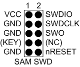
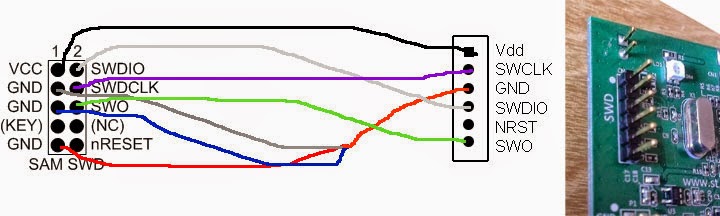
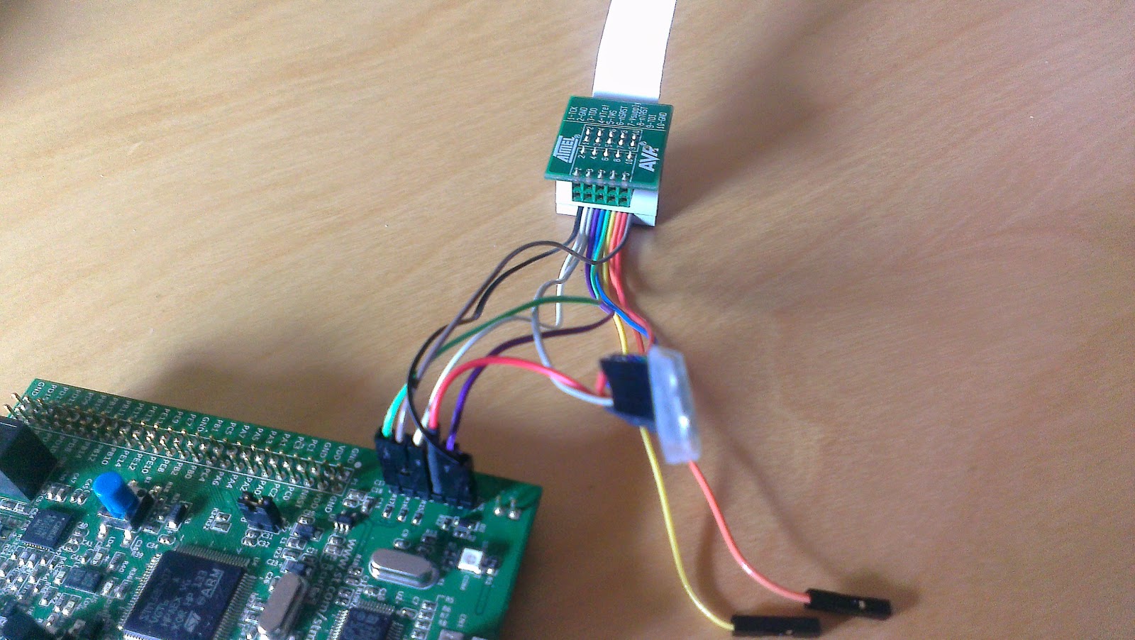
This is how you turn the Atmel ICE JTAG debugger into an STM32F4xx SWD debugger.
I used these two documents to figure out the pin assignments.
- USER MANUAL for Discovery kit for STM32F407/417 lines (page 14)
- Atmel ICE Physical Interface
First abortive attempt

So I connected it up as per the numbers, like this.
But these connections make no sense to me based upon what is written on the back of the 10-pin JTAG connector.
For example SWDIO on the SWD is linked to JTAG pin-2 which is GND.
I think my problem stems from the 10-pin AVR JTAG and the 10-pin ARM JTAG being different.

Second attempt – still under development
| SWD |
ARM JTAG |
AVR JTAG |
|
| 1 Vdd |
1 Vcc |
1 TCK |
|
| 2 SWCLK |
2 TMS |
2 GND |
|
| 3 GND |
3 GND |
3 TDO |
|
| 4 SWDIO |
4 TCLK |
4 VTref |
? |
| 5 NRST |
5 GND |
5 TMS |
|
| 6 SWO |
6 TDO |
6 RES |
|
|
7 RTCK |
7 Vcc |
|
|
8 TDI |
8 NC |
|
|
9 GND |
9 TDI |
|
|
10 RESET |
10 GND |
|
So maybe the connections should look like this.